- 您现在的位置:买卖IC网 > Sheet目录327 > HW-V5-ML561-UNI-G (Xilinx Inc)EVALUATION PLATFORM VIRTEX-5
Appendix C: LCD Interface
?
The voltage follower and voltage regulator are set to:
R
?
?
Five times boost mode
The V4, V3, V2, V1, and V0 outputs depend on the bias settings of 1/9 or 1/7.
Because of these default settings, the following display controller connections are not used:
?
?
?
?
DISP: Turns into an output when Master mode is selected
FRS: Static driver segment output
M: Used in Master/Slave display configurations
CL: Clock pin used in Master/Slave display configurations
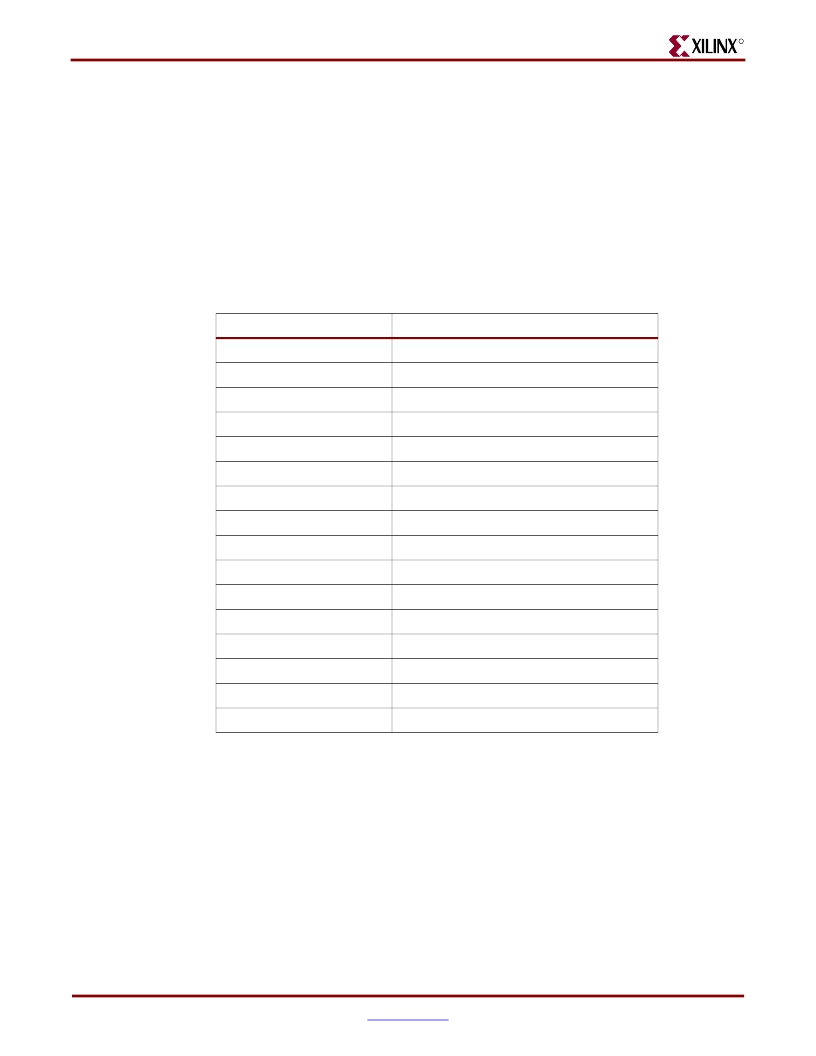
Table C-3:
Display Controller Initialization (RESETB is Low)
Parameter
Display
Entire Display
ADC Select
Reverse Display
Power Control
LCD Bias
Read-Modify-Write
SHL Select
Static Indicator Mode
Static Indicator Register
Display Start
Column Address
Page Address
Regulator Select
Reference Voltage
Reference Voltage Register
Initial Value
OFF
OFF
OFF
OFF
0,0,0 (VC, VR, VF)
1/7
OFF
OFF
OFF
0,0 (S1, S0)
0 (First line)
0
0
0,0,0 (R2, R1, R0)
OFF
1,0,0,0,0,0 (SV5, SV4, SV3, SV2, SV1, SV0)
When RESETB is High, the display must be initialized. The first steps to be taken to
guarantee correct operation of the display and the controller are:
?
Configure the ADC bit. This bit determines the scanning direction of the segments.
?
?
When the RESETB signal is active, ADC is reset to 0 , meaning that the segments
are scanned from SEG1 up to SEG132.
When ADC is set to 1 , the segments are scanned in opposite direction.
?
Configure the SHL bit. This bit sets the scanning direction of the COM lines.
?
?
When the RESETB signal is active, SHL is reset to 0 , meaning that the segments
are scanned from COM1 up to COM64.
When SHL is set to 1 , the common lines are scanned in opposite direction.
128
Virtex-5 FPGA ML561 User Guide
UG199 (v1.2.1) June 15, 2009
发布紧急采购,3分钟左右您将得到回复。
相关PDF资料
I-JET
JTAG ARM DEBUGGING PROBE
IAC24A
INPUT MODULE AC 5MA 24VDC
IAC5EQ
INPUT MODULE AC 10MA 5VDC
IB8RM
SURGE SUPP 8OUT 12'CORD W/REMOTE
IBAR12-20T
SURGE SUPPRSSR 20A 12OUT RACKMNT
IBAR12/20ULTRA
SURGE SUPPRSSR 20A 12OUT RACKMNT
IBAR12ULTRA
SURGE SUPPRSSR 15A 12OUT RACKMNT
IBAR12
SURGE SUPPRSSR 15A 12OUT RACKMNT
相关代理商/技术参数
HW-V5-ML561-UNI-G-J
功能描述:EVALUATION PLATFORM VIRTEX-5 RoHS:是 类别:编程器,开发系统 >> 通用嵌入式开发板和套件(MCU、DSP、FPGA、CPLD等) 系列:Virtex®-5 LXT 产品培训模块:Blackfin® Processor Core Architecture Overview
Blackfin® Device Drivers
Blackfin® Optimizations for Performance and Power Consumption
Blackfin® System Services 特色产品:Blackfin? BF50x Series Processors 标准包装:1 系列:Blackfin® 类型:DSP 适用于相关产品:ADSP-BF548 所含物品:板,软件,4x4 键盘,光学拨轮,QVGA 触摸屏 LCD 和 40G 硬盘 配用:ADZS-BFBLUET-EZEXT-ND - EZ-EXTENDER DAUGHTERBOARDADZS-BFLLCD-EZEXT-ND - BOARD EXT LANDSCAP LCD INTERFACE 相关产品:ADSP-BF542BBCZ-4A-ND - IC DSP 16BIT 400MHZ 400CSBGAADSP-BF544MBBCZ-5M-ND - IC DSP 16BIT 533MHZ MDDR 400CBGAADSP-BF542MBBCZ-5M-ND - IC DSP 16BIT 533MHZ MDDR 400CBGAADSP-BF542KBCZ-6A-ND - IC DSP 16BIT 600MHZ 400CSBGAADSP-BF547MBBCZ-5M-ND - IC DSP 16BIT 533MHZ MDDR 400CBGAADSP-BF548BBCZ-5A-ND - IC DSP 16BIT 533MHZ 400CSBGAADSP-BF547BBCZ-5A-ND - IC DSP 16BIT 533MHZ 400CSBGAADSP-BF544BBCZ-5A-ND - IC DSP 16BIT 533MHZ 400CSBGAADSP-BF542BBCZ-5A-ND - IC DSP 16BIT 533MHZ 400CSBGA
HW-V5-PCIE2-UNI-G
功能描述:KIT DEV PCIEXPRESS GTX VIRTEX5 RoHS:是 类别:编程器,开发系统 >> 通用嵌入式开发板和套件(MCU、DSP、FPGA、CPLD等) 系列:Virtex® -5 产品培训模块:Blackfin® Processor Core Architecture Overview
Blackfin® Device Drivers
Blackfin® Optimizations for Performance and Power Consumption
Blackfin® System Services 特色产品:Blackfin? BF50x Series Processors 标准包装:1 系列:Blackfin® 类型:DSP 适用于相关产品:ADSP-BF548 所含物品:板,软件,4x4 键盘,光学拨轮,QVGA 触摸屏 LCD 和 40G 硬盘 配用:ADZS-BFBLUET-EZEXT-ND - EZ-EXTENDER DAUGHTERBOARDADZS-BFLLCD-EZEXT-ND - BOARD EXT LANDSCAP LCD INTERFACE 相关产品:ADSP-BF542BBCZ-4A-ND - IC DSP 16BIT 400MHZ 400CSBGAADSP-BF544MBBCZ-5M-ND - IC DSP 16BIT 533MHZ MDDR 400CBGAADSP-BF542MBBCZ-5M-ND - IC DSP 16BIT 533MHZ MDDR 400CBGAADSP-BF542KBCZ-6A-ND - IC DSP 16BIT 600MHZ 400CSBGAADSP-BF547MBBCZ-5M-ND - IC DSP 16BIT 533MHZ MDDR 400CBGAADSP-BF548BBCZ-5A-ND - IC DSP 16BIT 533MHZ 400CSBGAADSP-BF547BBCZ-5A-ND - IC DSP 16BIT 533MHZ 400CSBGAADSP-BF544BBCZ-5A-ND - IC DSP 16BIT 533MHZ 400CSBGAADSP-BF542BBCZ-5A-ND - IC DSP 16BIT 533MHZ 400CSBGA
HW-VID-KIT
功能描述:可编程逻辑 IC 开发工具 Lattice Video Interface Kit
RoHS:否 制造商:Altera Corporation 产品:Development Kits 类型:FPGA 工具用于评估:5CEFA7F3 接口类型: 工作电源电压:
HW-VL1
制造商:IDEC CORPORATION 功能描述:BARRIER
HW-VL2
制造商:IDEC Corporation 功能描述:COVER;HW FNGR SAFE CONTAC CVR 制造商:IDEC CORPORATION 功能描述:HW FNGR SAFE CONTAC CVR
HW-VL3
制造商:IDEC Corporation 功能描述: 制造商:IDEC Corporation 功能描述:Replacs TW-VL3 FNGR SAF
HWW-X030T-10015Z-H1
制造商:P-TEC 制造商全称:P-tec Corporation 功能描述:X30T RGB LED Wall Washers
HWW-X030T-10015Z-H2
制造商:P-TEC 制造商全称:P-tec Corporation 功能描述:X30T RGB LED Wall Washers
